Introduction
This lab deals with the process of creating a $GaAsP$ LED which release red/orange light. Any semiconductor can be P-type or N-type depending on dopants used. N-type materials are doped so that there are free electrons that can move around in the crystal, while P-type materials have free holes.
When a P and N type semiconductor are in contact, electrons in the N-type material and holes in the P-type material flow to the junction until they combine. In certain PN junctions, the bandgap is indirect, meaning electron-hole recombination impart some angular momentum to the lattice atoms – heat. Other PN junctions, such as those of $GaAsP$, are direct bandgap semiconductors. An electron-hole recombination in these cases produce light and very little heat.
Procedure
First, safety precautions: Always wear protective eyewear (goggles or glasses) when working with chemicals, torches, or furnaces. Also, always wear gloves when handling acids/solvents, and make sure to wash hands immediately after handling them.
-
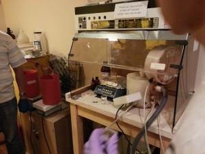
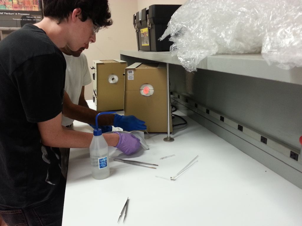
Put on gloves then wash tweezers with acetone and isopropyl alcohol. Always use tweezers or the chip box to handle to chip (do not touch it with your bear hands).
-
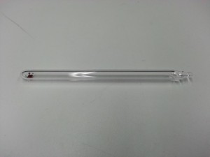
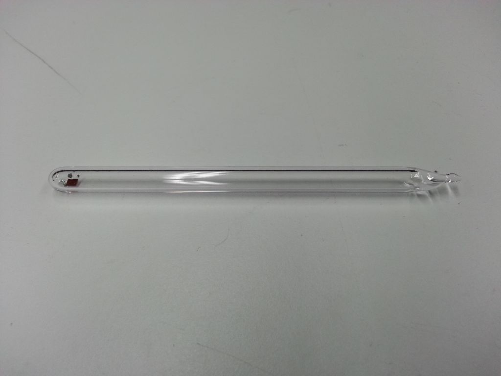
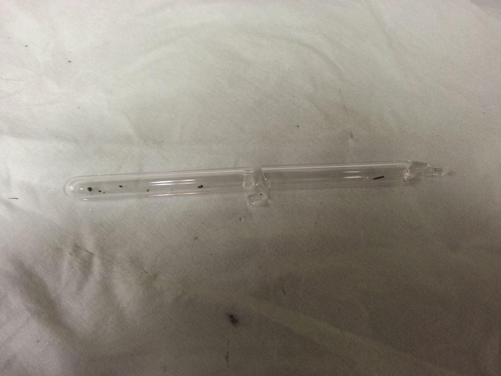
Place the chip (rough/back side down) along with a piece of $Zn_3As_2$ in a quartz tube. Heat the center of the tube with a torch and pump out the air, then seal it by twisting the tube shut. Cool the quartz in running water. Spin the tube until the $Zn_3As_2$ is at the other end.
-
Put the tube (chip first) into the center of the furnace. Leave there at $800^oC$ for 10 minutes. This will P-dope the $GaAsP$.
-

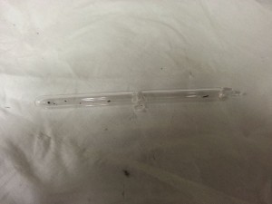
Grab the $Zn_3As_2$ end of the tube with a wet paper towel. This cools the tube which allows the As vapor to condense on it rather than the chip.
-
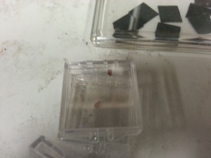
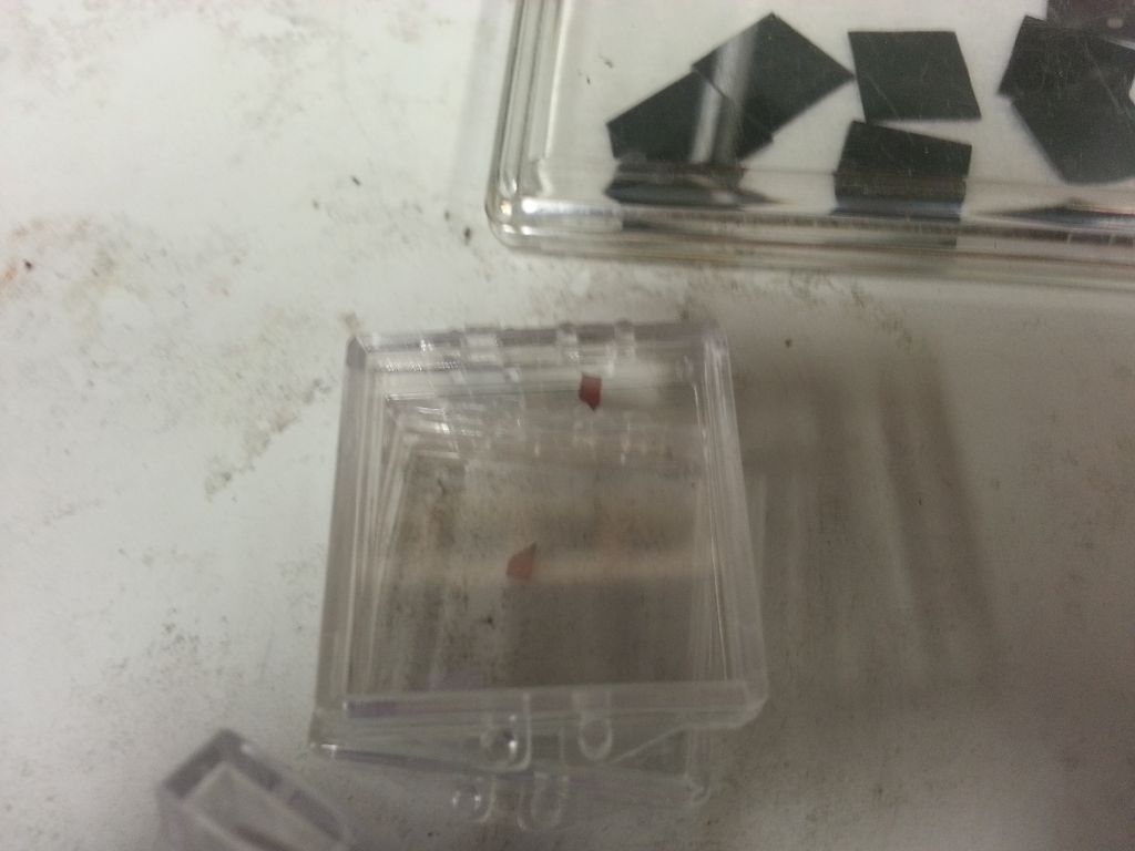
Score the tube along the middle to break it. Keep the LED chip in a chip box with your name.
-
Preheat a hotplate to $90^oC$ and mark a small dot on the shiny surface with a permanent marker (making sure it doesn’t touch the edge). Place the chip on the hotplate for one minute.
- Fill a small glass beaker half with $GaP$ etch and place it on the hotplate at $50^oC$ under the hood.
- Place the chip with wax dots in the etch for 4 minutes, then take it out and dip in into water and examine the chip to make sure it’s etched.
-
Squirt acetone onto the sample to remove the permanent marker. The etched mesas should be clearly visible. Rinse with isopropyl alcohol and blow the chip dry. The chip is ready for testing.

Results
The following procedure was followed to test the device:
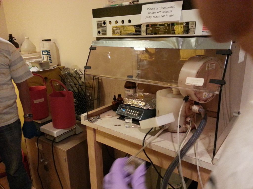
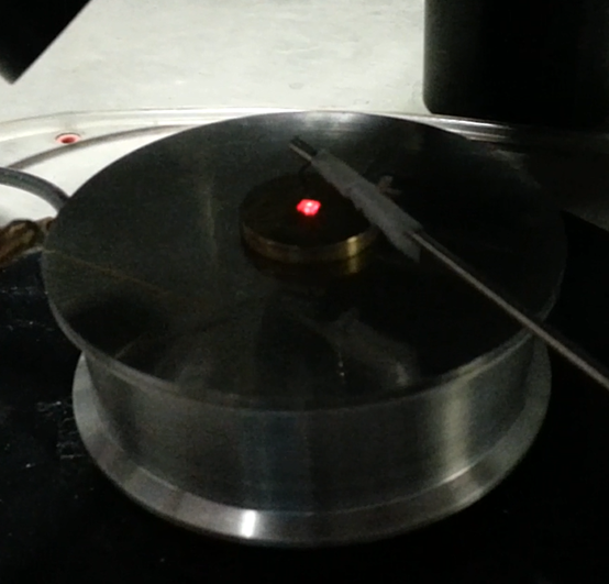
- Place the LED die on the vacuum plate of the analyzer and turn on the vacuum.
- Position the probe over the mesas of the die.
-
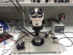
Turn on power to analyzer.
- Switch from channel page to softkey “MORE 1/2” and press MEM4 (Diode VF-IF) button.
- Set up channel definition menu with arrow bars. Press NEXT PAGE twice to reach measurement mode.
- Adjust voltage and current limits and step size. Ensure sweep is set up for single and linear sweep, with 40mA compliance. Use -5V to 5V to start.
- Press GRAPH button on console, then SINGLE. This will probe over a range of voltages over the LED. Press SCALING then AUTOSCALING if there’s no curve.
- Press PRINT/PLOT button, then PRINT/PLOT on the display, then hit YES.

Conclusion
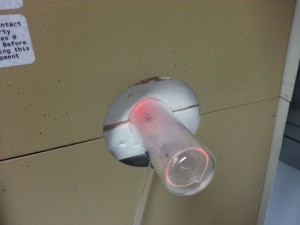
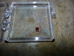
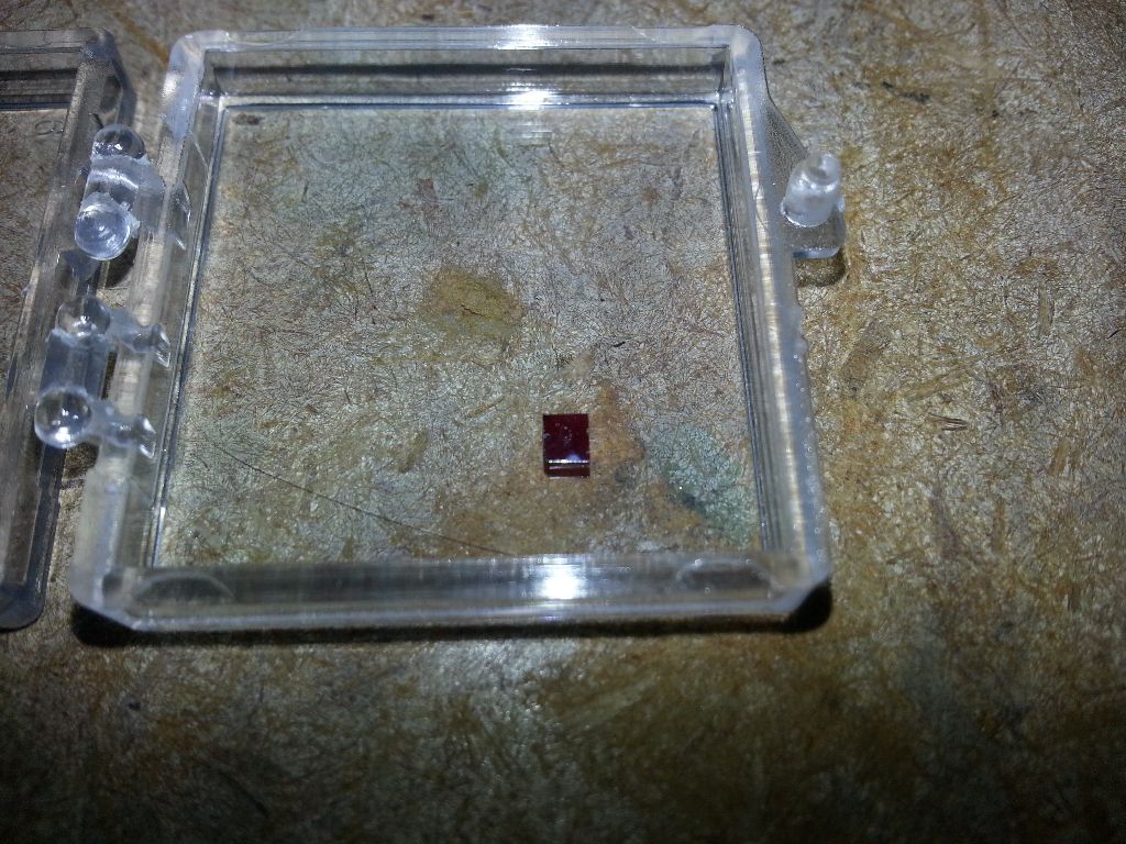
The procedure did produce a red LED that operated correctly (emitted light), as can be seen in the following image:
The following VI curve was created by testing the LED’s current at various voltages:
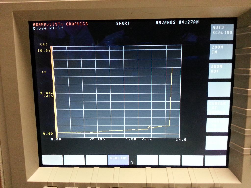
From this image, we can see the forward voltage was much higher than the bandgap for a red LED. The reason for this is probably due to some contamination, for example, from water. However, as the graph shows, once this forward voltage was reached, the current spiked.