However, we (or rather, our lab manual) screwed up. The process for making a MOSFET actually had us adding, then removing, the gate oxide. What this meant is we had direct contact to the N, P, and N regions – a very weak BJT.
Half of us ended up continuing with that, and half of us hadn’t etched the gate oxide, so were able to modify the process to create a MOSFET. Because both processes started from the same place, I’m going to include both in this lab.
Introduction
This lab creates both a MOS Field Effect Transistor (MOSFET) and a bi-junction transistor (BJT). The MOSFET is a device where the gate voltage with respect to the source pin voltage determines the drain-source conductance. The BJT is a device where the base-emitter voltage determines the collector current (it just so happens by coincidence that the base current is proportional to the collector current).
This lab utilizes techniques from the MOSCAP lab and the PN diode lab to produce three adjacent rectangular regions of N, P, and N-type silicon. For the BJT, contacts are created directly to these three regions via aluminum deposition, whereas for the MOSFET, a gate oxide is created before adding the contacts.
Procedure and Results
MOSFET/BJT Base
-
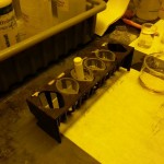
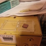
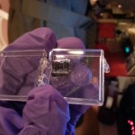
- Obtain a non-epitaxial P-type silicon chip.
-
- Place the chips in a boat and oxide etch.
-
- Rinse with acetone/IPA and air-blow-dry.
-
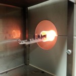
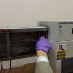
- Place the chips in a field oxide furnace at $1100^oC$ for 30 minutes.
-
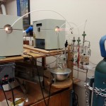
- Gas should be flowing through the water flask. The water should be hot.
-
- Remove the chips and place them on an aluminum block to cool.
-
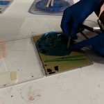
- Spin photoresist onto the chips.
-
- Apply the source/drain mask.
-
- Turn on the UV to expose the mask.
-
- Develop the photoresist.
-
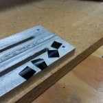
- After developing, masked regions are clearly visible.
-
- Etch the oxide region for 4 minutes away from the soruce/drain regions.
-
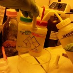
- Rinse with acetone and IPA to remove any remaining photoresist.
-
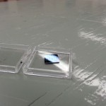
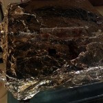
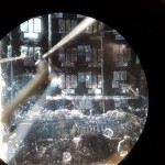
- Etched chip. lighter regions are exposed silicon next to the darker oxide regions.
-
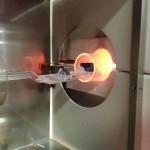
- Place the chips in a boron furnace at $950^oC$ for 30 minutes to dope the source/drain regions N-type.
-
- Spin more photoresist onto the chips.
-
- Chip with a thin layer of photoresist.
-
- Find a good source/drain region on the chip.
-
- Position the gate mask over the center of the source/drain regions/
-
- After exposing the photoresist and developing it, apply another oxide etch for 4 minutes.
-
- Rinse with acetone/IPA to remove leftover photoresist.
-
- Grow the gate oxide region at $1000^oC$ (first at $1 ft^3/hr O_2$ for 30 minutes, then $N_2$ for 10 minutes.
-
- Remove the chips and place them on an aluminum block to cool.
-
- Spin more photoresist, and…
-
- …bake the chips.
Completing the MOSFET
-
- Apply the contact (aluminum deposition) mask.
-

- UV expose for 1.5 minutes.
-
- Develop the photoresist.
-
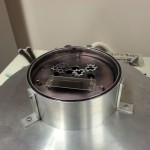
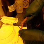
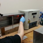
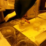
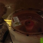
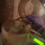
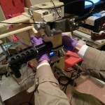
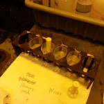
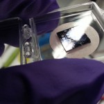
- Place the chips (photoresist-down) onto the aluminum deposition chamber grate. Run the machine to apply a thin aluminum contact.
-

- Gently remove the photoresist in acetone to get rid of unwanted aluminum, leaving aluminum in just the contact areas.
-
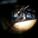
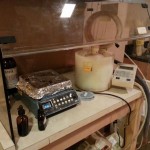
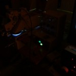
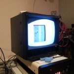
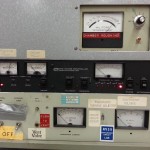
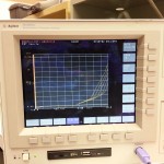
- Place the chip in the analyzer and place probes onto the three contact regions of the MOSFET.
-
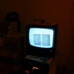
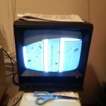
- Running the analyzer shows a characteristic MOSFET $I_D$ vs $V_{DS}$ curve.
Completing the BJT
-

- Apply the contact mask.
-
- UV-expose the photoresist.
-
- Chip after exposure.
-
- Develop the photoresist.
-
- Oxide etch away the gate oxide we’d added earlier (woops).
-
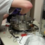
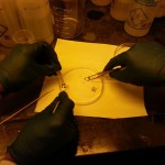
- Prepare the aluminum deposition chamber.
-

- Place the chips, photoresist-down onto the grate.
-
- Bring the vacuum down…
-
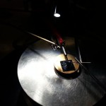
- …and engage the fine vacuum pump, then run a current through the titanium wire to vaporize the aluminum.
-
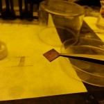
- Remove non-contact aluminum by gently swirling the chip in acetone.
-
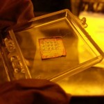
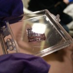
- Metalized chip.
-
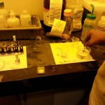
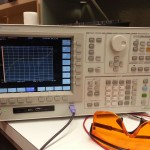
- Place the chip on the analyzer.
-
- Apply probes to the three regions – base, collector, emitter. In this device, the collector and base regions may have had slight contact due to mask misalignment.
-
- Running the analyzer shoes curves characteristic of a diode-connected transistor where the collector and base are connected together.